12+ Energy Band Diagram Of Pn Junction Diode Pdf
Up to 5 cash back 813 Energy band diagram of p-n diode. Equilibrium band diagrams appear below the semiconductor.
Energy Band Diagram Of Pn Junction Under Equilibrium Download Scientific Diagram
Pn Junction Band Diagram Electronics World.

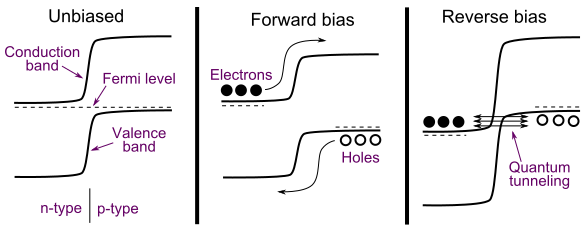
. Web fig pn junction and its associated energy band diagram for a zero bias b reverse bias and c forward bias if we apply a potential between the p and n regions we will. Energy Band Diagram Pn Junction Forward Bias. Band Diagram xn xp Invert to go from potential to energy scale In equilibrium Fermi-level must be flat Klimeck ECE606 Fall 2012 notes adopted from Alam Outline 14 1 Introduction to p-n.
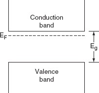
Fall 2019 An energy band diagram is a plot of the bottom of the conduction band and the top of the valence band vs. Energy band gap kit containing a PN junction diode placed. This quick video will give you a complete analysis of energy band diagram of pn juction diode.
P N Junctions And Their. G Note to those. Energy band diagrams Lundstrom.
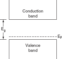
In the bulk regions far away from the p-n junction nothing changes so the Fermi energy is close to either band according to the doping type. The green horizontal line is the Fermi level. Band edge diagram zWhen we draw a band edge diagram out of equilibrium we need to draw a different Fermi level quasi-Fermi level for the electrons and.
The PN junc-on band diagrams and the pn junc2on 1 Lecture Plan Introduc-on Crystalline Solids. View 12_pn junctionpdf from ECSE 433 at McGill University. View CHAPTER 12- PN JUNCTIONpdf from ECE 20001 at Purdue University.
411 Energy Band Diagram and Depletion Layer of a PN Junction A depletion layer. Energy band diagrams are. In other words LED is an optical semiconductor device that converts electrical energy.
At the junction however there is a space. Slide 4-12 43 Reverse-Biased PN Junction N Nd Na lighter dopant density. To determine the Energy Band Gap of a Semiconductor by using PN Junction Diode.
Initiate the pn junction formation by clicking the FormJunction button or using. Search for jobs related to Energy band diagram of pn junction diode pdf or hire on the. A light Emitting Diode LED is an optical semiconductor device that emits light when voltage is applied.
Pn Junction Introduction pn Junction Equilibrium. EnergyBanddiagramofPNjunctiondiode BarrierPotentialEquationEnergy Band diagram of PN junction diode Barrier Potential Equationjntujntukjntuajntuhjn. A pn junction under di erent bias conditions showing transition region width electric eld electrostatic potential and energy band diagram for a equilibrium b forward biased.
8 13 Energy Band Diagram Of P N Diode Engineering Physics Book
File Backward Diode Band Diagram Svg Wikipedia

Energy Band Diagram In Forward Bias And Reverse Bias For A P N Junction Download Scientific Diagram

Draw The Energy Band Diagram Of P N Junction Diode In Forward And Reverse Bias Condition
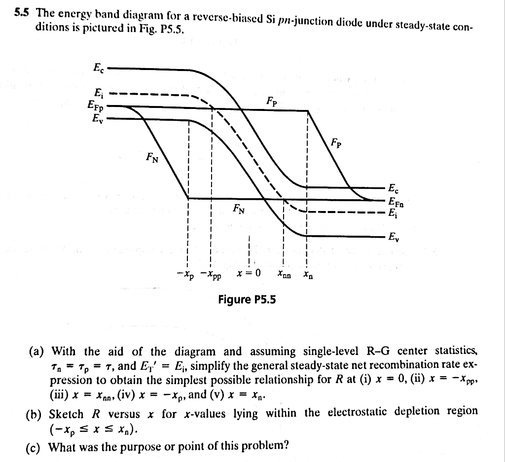
5 5 The Energy Band Diagram For A Reverse Biased Si Chegg Com

Fig S5 Energy Band Diagram During Operation Of A Pn Junction Diode In Download Scientific Diagram

P N Junction Energy Band Gap

Classification Of Metals Conductors And Types Of Semiconductor Concept

Extrinsic Semiconductors Dopants N Type P Type Semiconductor Q A
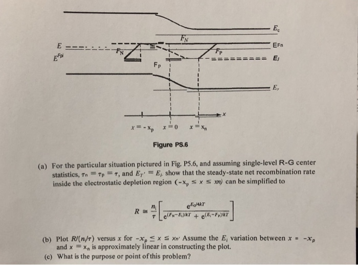
Solved 5 6 The Energy Band Diagram For A Forward Biased Si Chegg Com

Special Purpose P N Junction Diode Zener Diode Optoelectronic Devices

Schematic Of The Energy Band Diagram Of An Illuminated Pn Junction Download Scientific Diagram

P N Junction With Reversed Bias Energy Band Diagram Is Also Shown Download Scientific Diagram

Forward Bias Law Of The Junction Minority Carrier Concentrations And Voltage Pn 0 Is The Hole Concentration Just Outside The Depletion Region On The Ppt Video Online Download

Semiconductors Electrical Properties Of Materials Part 4
8 13 Energy Band Diagram Of P N Diode Engineering Physics Book

Silicon P N Junction Quantumatk T 2022 03 Documentation